Printed circuit board (PCB)
Carrier responsible for the mechanical and electrical connection of electronic components
Request a demo
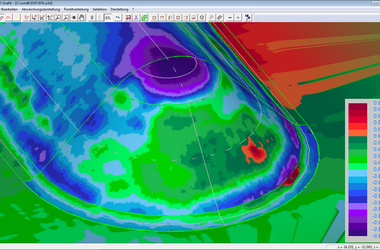
The key geometric characteristics of printed circuit boards (PCBs) are the distances between hole patterns and electrical components within a single plane. Bond-wire continuity, solder-joint defects, and other defects are also inspected. With tolerances from 20 µm to 50 µm, measurement-uncertainty requirements are moderate, while measurement-time requirements are very high.
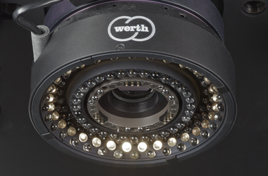
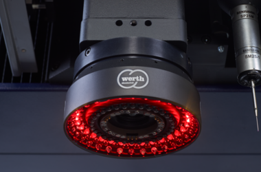
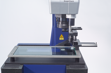
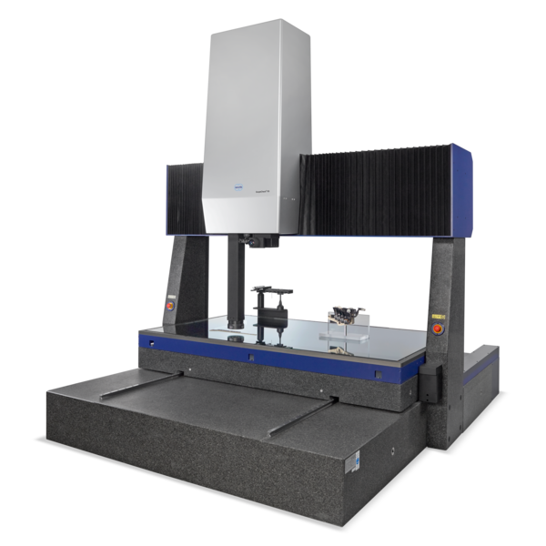
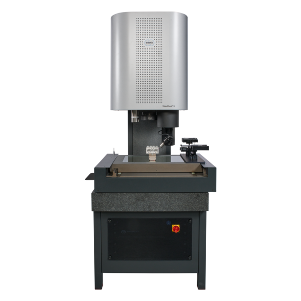
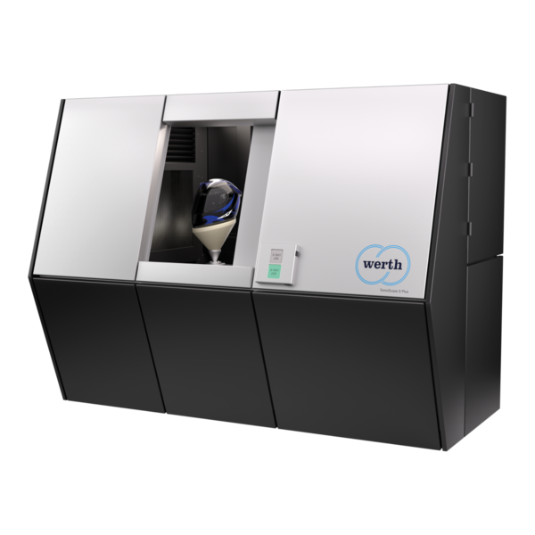
A FlatScope 2D scanner is suitable for high-speed inspection of large flat panels, while the multisensor ScopeCheck® S is used for precise geometry and defect inspection. CT-based inspection is effective for evaluating internal joints and layered structures.
Recommended systems